Nanophysics: The Right Twist
29 March 2023
Nanophysics: The Right Twist
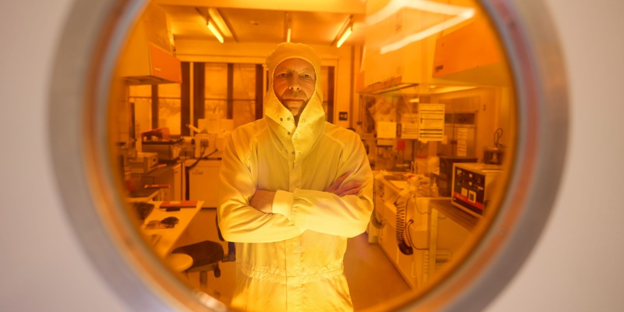
Stacked layers of ultrathin semiconductor materials feature phenomena that can be exploited for novel applications. A team led by LMU physicist Alexander Högele has studied effects that emerge by giving two layers a slight twist.
Novel, ultrathin nanomaterials exhibit remarkable properties. If you stack individual atomically thin layers of crystals in a vertical assembly, for example, fascinating physical effects can occur. For instance, bilayers of the wonder material graphene twisted by the magic angle of 1.1 degrees may exhibit superconductivity. And researchers are also focusing their attention on bilayer semiconducting heterostructures made of so-called transition metal dichalcogenides, which are held together weakly by van der Waals forces.
The research group led by Alexander Högele investigates such novel heterostructures, which do not occur in nature. “The combination of materials, the number of layers, and their relative orientation give rise to a wide variety of novel phenomena,” says the LMU physicist. “In the lab, we can tailor physical phenomena for various applications in electronics, photonics, or quantum technology with properties that are unknown in naturally occurring crystals.” Experimentally observed phenomena are not always easy to interpret, however, as a new paper published in the journal Nature Nanotechnology demonstrates.
Moiré effects depend on the orientation of the layers
Högele’s team investigated a heterobilayer system held together by van der Waals forces and fabricated from semiconductor monolayers of molybdenum diselenide (MoSe2) and tungsten diselenide (WSe2). Depending on the orientation of the individual layers, moiré effects can emerge. These effects, which we are familiar with from everyday life, also arise in the nano-world when two different atomic lattices are stacked upon each other, or two identical lattices are twisted with respect to each other. The difference in the nano case is that it is not an optical effect. In the quantum mechanical world of atomically thin crystal heterostructures, moiré interference dramatically affects the properties of the composite system, also impacting electrons and strongly bound electron-hole pairs, or excitons, explains Högele.
“Our work shows that the naïve notion of a perfect moiré pattern in heterobilayer MoSe2-WSe2 does not necessarily hold true, particularly for small angles of rotation. Therefore, the interpretation of the phenomenology observed to date will have to be partially revised,” says Högele. Instead of periodic moiré patterns, there are laterally extended areas that are free from moiré interferences. Moreover, there are zones with interesting quantum mechanical effects such as one-dimensional quantum wires or quasi zero-dimensional quantum dots that are potentially viable for applications in quantum communication based on spatially localized excitons with single-photon emission characteristics. In the latter case, ideal moiré patterns presumably transform into periodic patterns with triangular or hexagonal tiling.
Collective phenomena in synthetic crystals
The reason seems to lie in an elastic deformation of the lattice structure that depends on the orientation of the layers. The atoms are displaced out of their equilibrium positions, which comes at the expense of increased strain in individual layers but promotes better adhesion among the layers. The result is an energy landscape in the heterobilayer system that can be engineered and potentially exploited by means of rational design. “We also observe collective phenomena in synthetic crystals, where periodic moiré patterns have a dramatic effect on the motion of electrons as well as their mutual interactions,” says Högele.
Of decisive importance is the understanding of excitons –electron-hole pairs – that are characteristic for the distinct types of atomic registries in bilayer crystal heterostructures and which could potentially be utilized in future opto-electronic applications. These excitons are generated in semiconducting transition metal dichalcogenides by means of light absorption, and convert back into light again. “Excitons thus act as mediators of light-matter interaction in semiconductor crystals,” says Högele. As the current paper shows, different types of excitons arise depending on the actual structure of the heterobilayer systems in parallel or antiparallel alignment. “We want to learn how to manufacture van der Waals heterostructures with customized properties in a deterministic approach to control the rich emergent phenomenology of correlated effects such as magnetism or superconductivity.”
Source: LMU Website
Publication
Excitons in mesoscopically reconstructed moiré heterostructures.
S. Zhao, Z.Li, X. Huang, A. Rupp, J. Göser, I. A. Vovk, S. Yu. K., K.Watanabe, T.Taniguchi, I.Bilgin, A.S. Baimuratov & A. Högele.
Nature Nanotechnology (2023)
DOI: 10.1038/s41565-023-01356-9